Possion’s Equation (simple)
- Using in the above equation and rearranging allows xp and xn to be determined. They are:
- From these equations we can get the maximum electric field: ,
- and the total width of the depletion region.
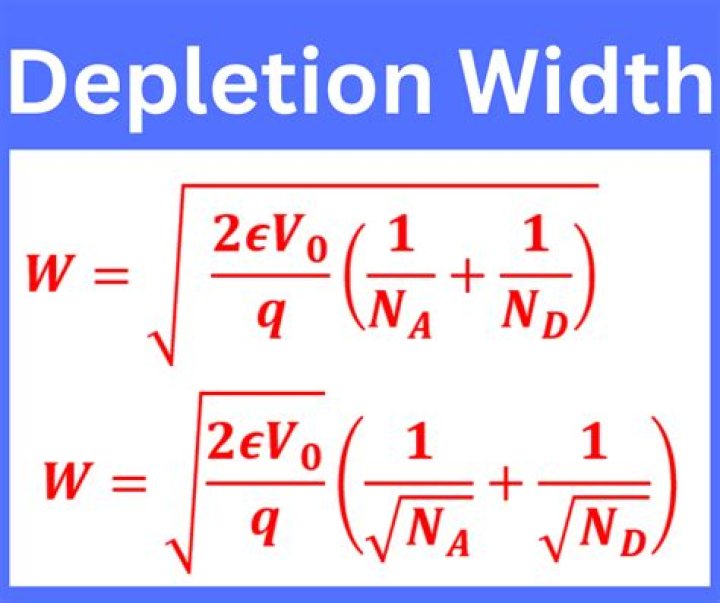
- W = x p + x n = 2 ε q V o ( 1 N A + 1 N D )
- and.
What is in Shockley equation?
Is=reverse bias saturation current (A) A=empirical constant needed for practical diodes ≈ 2. qe=electron charge ≈ 1.602×10⁻¹⁹ C. V=applied forward bias (V)
What is Shockley equation in electronics?
Derivation. Shockley derives an equation for the voltage across a p-n junction in a long article published in 1949. the difference between the quasi-Fermi level of the holes at the junction and that of the electrons at the junction. the drop of the quasi-Fermi level of the electrons from the junction to the n terminal.
What is the diode current equation?
Diode Equation at Room Temperature Let the room temperature is 27°C. The ratio KT/q is called the thermal voltage of the diode.
What is depletion width of pn junction diode?
The physical width of the depletion region in a typical Si diode ranges from a fraction of a micrometer to tens of micrometers depending on device geometry, doping profile, and external bias. Figure 11.4. Simplified representation of a pn-junction.
What is ideality factor of Schottky diode?
Ideality factor of 0.4 for a Schottky diode.
What is the value of VT in diode equation?
Why is Vt usually 26 mV in the diode formula? – Electrical Engineering Stack Exchange.
Is Shockley equation linear?
One simple method is using linear graphical fit at zero current or voltage conditions. The fittings were performed using the nonlinear equation of Shockley by determining some initial values of fittings such as Rs, Rsh, n, I0, Iph, and T.
How do you calculate the value of a diode?
Diode Resistance Formula Diode resistance is equal to the thermal voltage, VT, divided by the current, Id, passing through the diode. The thermal voltage of the diode is approximately 25mV at 300K, which is a temperature that is very close to room temperature.
How do you calculate the width of the depleted p-type region?
The width of the depleted p-type region (which is left negatively charged): x 2ε p( = r ε0 V biN D q N AN A +N
What is depletion region?
The region in the vicinity of the junction, which has been depleted of the free charge carriers is called “depletion region”. The width of the depletion region is: V W 2ε D=r
How do you find the electric field of a depletion region?
The electric field is obtained by integrating equation (4.3.9). The boundary conditions, consistent with the full depletion approximation, are that the electric field is zero at both edges of the depletion region, namely at x = -x p and x = x n.
What are the boundary conditions for full depletion approximation?
The boundary conditions, consistent with the full depletion approximation, are that the electric field is zero at both edges of the depletion region, namely at x= -xpand x= xn. The electric field has to be zero outside the depletion region since any field would cause the free carriers to move thereby eliminating the electric field.