The critical path is defined as the path between an input and an output with the maximum delay. Once the circuit timing has been computed by one of the techniques listed below, the critical path can easily be found by using a traceback method.
What is critical path in VLSI design?
The critical path is the longest path in the circuit and limits the clock speed. Latency is the time needed for an input change to produce an output change; latency can be expressed as a length of time or, in synchronous circuits, as a certain number of clock cycles.
How many types of timing paths are possible in a design?
If we use all the combination of 2 types of Starting Point and 2 types of End Point, we can say that there are 4 types of Timing Paths on the basis of Start and End point. Input pin/port to Register(flip-flop).
What is tpd in digital electronics?
The time interval between specified reference points on the input and output voltage waveforms with the output changing from one defined level (high or low) to the other defined level.
What is the critical path delay?
The critical path delay is the sum of the delays of the shifter, the conditional complementer (for the subtraction), the adder, and the register.
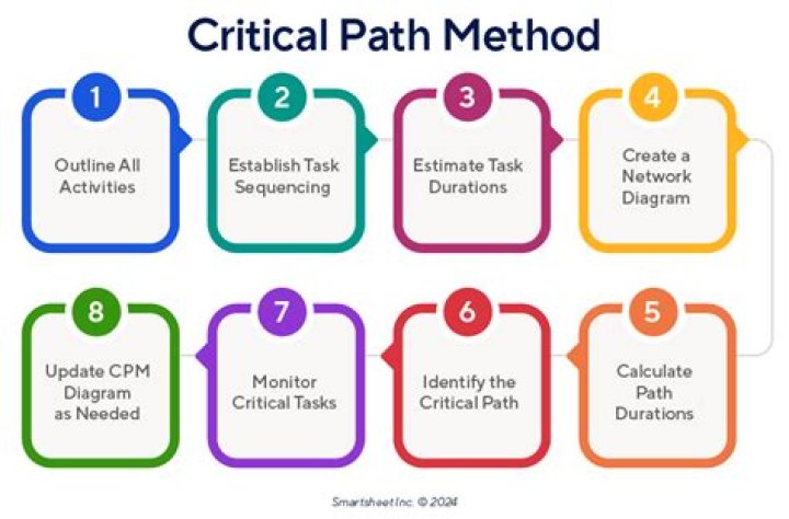
How is the critical path calculated?
How to manually calculate critical path in project management. Identify all possible paths through the diagram, and add up all tasks’ duration to calculate the time to complete each path. The path that has the longest total duration is your critical path.
What are timing paths in VLSI?
Timing path is defined as the path between start point and end point where start point and end point is defined as follows: Start Point: All input ports or clock pins of a sequential element are considered as valid start point.
Why is timing important in VLSI?
During designing there is a trade-offs between speed, area, power, and runtime according to the constraints set by the designer. However, a chip must meet the timing constraints to operate at the intended clock rate, so timing is the most important design constraint.
What is timing paths in VLSI?
Timing path is defined as the path between start point and end point where start point and end point is defined as follows: Start Point: All input ports or clock pins of a sequential element are considered as valid start point. End Point: All output port or D pin of sequential element is considered as End point.
What is STA timing path?
STA also considers the following types of paths for timing analysis: Clock path. A path from a clock input port or cell pin, through one or more buffers or inverters, to the clock pin of a sequential element; for data setup and hold checks. Clock-gating path.
What is TPD and TCD?
∎ Contamination delay (tcd. ): delay until Y starts changing. ∎ Propagation delay (tpd. ): delay until Y finishes changing.
Which flipflop is used as a latch?
Correct Option: B. RS flip-flop is used as a latch.
What are the different types of timing critical paths?
They can be divided into setup and hold timing critical paths. Setup timing critical paths: Those paths for which meeting setup timing is difficult, can be termed as setup critical timing paths. For these paths, the setup slack value is very close to zero and for the most part of design cycle, remains below zero.
What is critical path in circuit?
•Critical Path: the path in the entire design with the maximum delay. – This could be from state element to state element, or from input to state element, or state element to output, or from input to output (unregistered paths). • For example, what is the critical path in this circuit?
How do I create a category for a timing path?
You can add two “conditions” together to create more complex searches of the timing paths to find commonality. It’s fun (and very useful). Click on the “Create” button on the button of the page to run and create the category. Add the category to your histogram view to see how widespread the category is amongst the critical paths in your design.
What maximum frequency does the timing path need to work?
Let us check at what maximum frequency our timing path will work. First, we need to ensure hold timing is met. Thus, This translates to Combinational delay (Cb) > 100 ps, or Cb = 100 ps for a hold slack of 0 ps. In other words, worst case combinational delay is 200 ps (2 times scaling).